
1 /
4
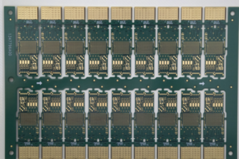
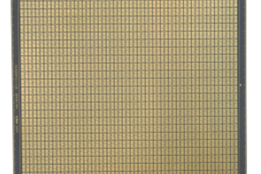
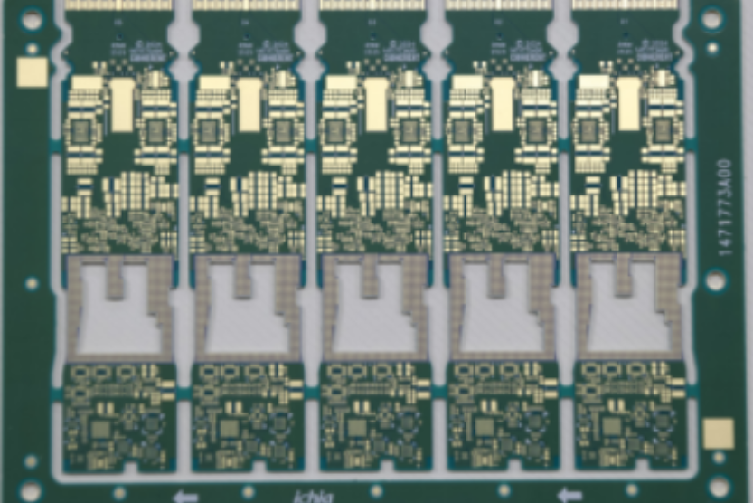

SLP (Substrate-like PCB)
Description:
Key Capabilities & Services Offered
- Supports 3-layer, 6-layer, and multilayer boards (primarily 8–16 layers)
- Laser via: minimum 35μm; blind via: minimum 50μm
- Microvia filling and any-layer interconnection technology
- Circuit capability: 20μm/20μm line width/spacing
- Solder mask ink exposure accuracy: ±25μm
- Advanced mSAP + HDI + core-less technology for high-end applications
- Complete one-stop service from any-layer manufacturing to testing, inspection, and packaging
SLP (Substrate-like PCB) is an advanced form of PCB that offers significantly finer line and space capabilities, closely resembling semiconductor packaging substrates. It is primarily adopted in high-end smartphones and optical fiber communication solutions where ultra-high density, superior electrical performance, and compact design are essential. We provide end-to-end SLP services—from manufacturing and flip chip processing to testing, inspection, and packaging—ensuring precision, reliability, and optimal performance for next-generation applications.
